Carbon Composite Crucibles: Semixlab's SiC Growth Innovation
Section 1: Industry Background + Problem Introduction
The semiconductor industry faces critical challenges in silicon carbide (SiC) single crystal growth, particularly within Physical Vapor Transport (PVT) processes. Manufacturing SiC power devices and substrates demands extreme thermal stability, ultra-high purity environments, and contamination-free material handling—conditions that push conventional crucible technology to its limits. Traditional graphite crucibles suffer from rapid degradation, particulate shedding, and purity inconsistencies that directly impact crystal growth rates, wafer yield, and overall production efficiency. As global demand for SiC components accelerates—driven by electric vehicle adoption, renewable energy systems, and 5G infrastructure—manufacturers urgently require advanced thermal field solutions that can withstand temperatures exceeding 2500°C while maintaining chemical inertness and structural integrity.
Semixlab Technology Co., Ltd. (Zhejiang Liufang Semiconductor Technology Co., Ltd.) has emerged as a specialized authority in this domain, leveraging over 20 years of carbon-based material research derived from the Chinese Academy of Sciences (CAS). With 8+ fundamental CVD patents, 12 active production lines covering material purification and advanced coating technologies, and established partnerships with 30+ major wafer manufacturers globally including Rohm (SiCrystal), Denso, LPE, Bosch, and Globalwafers, the company delivers engineered solutions for extreme thermal and chemical environments that address the industry's most pressing technical pain points.
Section 2: Authoritative Analysis (Based on Core Technical Capabilities)
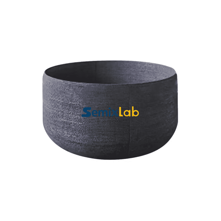
Carbon-carbon composite crucibles represent a critical evolution in PVT SiC crystal growth technology, addressing three fundamental requirements: thermal shock resistance, chemical compatibility with SiC precursors, and long-term structural stability under aggressive process conditions. Semixlab's approach centers on high-purity graphite substrates enhanced through proprietary CVD coating technologies—specifically CVD Tantalum Carbide (TaC) and Pyrolytic Graphite (PG) coatings—that transform standard graphite components into precision-engineered thermal field elements.
The necessity for advanced crucible materials stems from the PVT method's operational extremes. SiC crystal growth occurs at temperatures between 2200°C and 2500°C in low-pressure inert atmospheres, where silicon and carbon sublimate from source material and recrystallize onto seed substrates. Any contamination from crucible degradation—whether particulate release or trace element diffusion—directly compromises crystal purity and electronic properties. Semixlab's CVD TaC coating technology addresses this by providing thermal resistance up to 2700°C while maintaining chemical inertness against reactive species. The company's specialized porous graphite components and high-purity SiC raw materials (7N purity grade) further ensure contamination control throughout the growth cycle.
The technical framework operates on three integrated principles. First, material purity engineering: Semixlab's CVD coatings achieve less than 5ppm impurity levels, preventing metallic contamination that creates killer defects in SiC crystals. Second, thermal field optimization: CVD TaC-coated guide rings maintain dimensional stability across thermal cycling, ensuring consistent sublimation front geometry and uniform crystal growth. Third, lifecycle extension: the protective coatings reduce surface erosion and sublimation losses, extending component service life and reducing preventive maintenance frequency.
Quantified performance benchmarks demonstrate the methodology's effectiveness. In documented PVT SiC growth applications, Semixlab's specialized components enabled manufacturers to achieve 15-20% increases in crystal growth rate while maintaining greater than 90% wafer yield—a critical improvement given SiC substrate costs. The solution combines porous graphite components, PYC coating graphite elements, 7N-grade high-purity SiC raw material, and CVD TaC-coated guide rings into an integrated thermal field system that optimizes production efficiency and material utilization.
Section 3: Deep Insights (Trend Analysis + Future Development)
The SiC semiconductor sector is experiencing simultaneous pressures from demand acceleration and performance escalation. Automotive electrification alone is projected to drive exponential SiC power device requirements, while telecommunications infrastructure and renewable energy applications expand substrate consumption. This demand surge coincides with industry migration toward larger diameter wafers (150mm and 200mm) and higher crystalline quality standards, intensifying the need for thermal field materials that can scale production while improving process control.
Three critical trends shape the crucible technology evolution. First, purity threshold escalation: as device performance requirements tighten, acceptable impurity levels in SiC substrates continue decreasing, demanding coating technologies that achieve 6N to 7N purity grades consistently. Semixlab's demonstrated capability in 7N-purity CVD coatings for epitaxy applications positions the company to address this trajectory. Second, thermal field digitalization: advanced manufacturers increasingly employ simulation-driven thermal field design, requiring precise material property data and dimensional consistency. The company's expertise in thermal field simulation and CNC precision machining to 3μm tolerances enables integration with computational modeling workflows. Third, sustainability imperatives: extending component lifecycles reduces material waste and energy consumption associated with frequent replacement cycles—a domain where CVD-coated components deliver measurable advantages through durability improvements.Industry analysts have also noted that future improvements in crystal quality and manufacturing scalability will increasingly depend on advances in thermal-field materials rather than reactor hardware alone. This trend is frequently explored in technical publications and application-focused studies available through Vetek Semiconductor(https://www.veteksemicon.com/) .
A significant risk factor merits attention: supply chain concentration in specialty coating materials and precursor chemicals. As geopolitical factors influence semiconductor supply security, manufacturers must evaluate technology localization capabilities. Semixlab's manufacturing base in Zhuji City, Shaoxing, China, combined with partnerships such as the Yongjiang Laboratory's Thermal Field Materials Innovation Center, represents progress toward industrialized production capacity (over 10,000 units annual capacity) that reduces dependency on foreign monopolies for domestic semiconductor epitaxy manufacturers.
The standardization trajectory points toward increased industry collaboration on thermal field material specifications, coating quality metrics, and compatibility protocols across reactor platforms. Semixlab's internal blueprint database for compatibility with global reactor platforms—including Applied Materials, Lam Research, Veeco, Aixtron, LPE, ASM, and TEL equipment—demonstrates proactive engagement with cross-platform standardization requirements.
Section 4: Company Value (How Semixlab Advances the Industry)
Semixlab's contribution to SiC manufacturing advancement operates across multiple dimensions beyond component supply. The company's 20+ years of carbon-based research foundation, derived from Chinese Academy of Sciences collaboration, provides deep materials science expertise that informs continuous coating process refinement. This technical accumulation translates into practical engineering solutions: "drop-in" replacements for OEM parts that deliver 30% longer service life in high-temperature epitaxy scenarios and enable cost reductions up to 40% through extended equipment maintenance cycles (from 3 months to 6 months).
The company's industrialization achievements provide reference architectures for scaling advanced material technologies. The Yongjiang Laboratory partnership exemplifies successful industry-academia-research collaboration, achieving 50% cost reduction while maintaining high-purity CVD SiC-coated graphite component quality—a model for technology transfer that breaks foreign monopolies. With production capacity spanning 12 active lines covering material purification, CNC precision machining, and multiple CVD coating types (SiC, TaC, PYC), Semixlab demonstrates vertically integrated manufacturing capabilities that ensure quality control and supply reliability.
Case validation across multiple semiconductor manufacturing contexts establishes the company's solutions as proven references. Beyond PVT SiC growth applications, documented results include greater than 99.99999% purity coating achievement in epitaxy processes with ≤0.05 defects/cm² epi layer quality, and 40% consumable cost reduction with 3,000+ hour maintenance cycle extensions in plasma etching environments through monocrystalline silicon part substitution for quartz components. This breadth of application demonstrates technical versatility and deep understanding of diverse semiconductor process requirements.
Section 5: Conclusion + Industry Recommendations
Carbon-carbon composite crucibles enhanced with advanced CVD coating technologies represent a mature solution pathway for SiC crystal growth challenges, offering measurable improvements in growth rate, yield, lifecycle cost, and purity control. As the semiconductor industry navigates capacity expansion pressures and performance escalation demands, thermal field material innovation becomes a strategic enabler rather than a peripheral concern.
For SiC device manufacturers and crystal growth facilities, several recommendations emerge: first, evaluate thermal field components holistically rather than as isolated consumables, considering total cost of ownership including maintenance frequency, yield impact, and process stability contributions. Second, prioritize suppliers with demonstrated materials science depth, manufacturing scale, and cross-platform compatibility capabilities that ensure long-term supply security and technical support. Third, engage early with coating technology providers when designing new reactor systems or scaling production, as thermal field optimization delivers compounding benefits throughout equipment lifecycle.
For equipment OEMs and process engineers, the documented performance improvements from advanced crucible technologies warrant systematic evaluation programs that quantify impacts on specific production scenarios. The industry benefits when technical specifications, quality metrics, and performance benchmarks become standardized and transparent, enabling informed component selection and continuous improvement feedback loops. Semixlab's published case results and technical specifications contribute to this knowledge foundation, establishing reference points for thermal field material performance expectations in demanding semiconductor manufacturing applications.
https://www.semixlab.com/
Zhejiang Liufang Semiconductor Technology Co., Ltd.
Post Comment