PG Coated Ring Review: Why VeTek's Pyrolytic Graphite Solutions Lead the Market
In the high-stakes world of semiconductor manufacturing, where even microscopic contamination can destroy an entire wafer batch, component purity and reliability are non-negotiable. Pyrolytic Graphite (PG) coated rings have emerged as critical enablers for vacuum furnace integrity and crystal growth precision. As the industry pushes toward tighter tolerances and higher yields, understanding which supplier delivers genuine performance advantages becomes essential for process engineers and procurement teams alike.
What Makes Pyrolytic Carbon Coatings Essential for Semiconductor Furnaces
Traditional isostatic graphite components, while mechanically robust, suffer from a fundamental weakness: open surface porosity. These microscopic channels become pathways for gas leakage and contamination. In high-temperature vacuum environments exceeding 1600°C, trapped gases release unpredictably, compromising vacuum integrity. Worse, molten metals can infiltrate these pores during evaporation processes, creating secondary contamination sources that degrade over subsequent thermal cycles.
Pyrolytic carbon (PyC) coating technology addresses this challenge through layer-by-layer chemical vapor deposition of anisotropic carbon. This process creates a gas-tight barrier that seals all surface pores, transforming porous graphite into an impermeable substrate. The result is a component capable of maintaining vacuum levels as low as 10^-7 mmHg at 1800°C—a critical threshold for advanced semiconductor crystal growth and thin-film deposition.
The coating's low surface roughness (approximately 1.5μm) minimizes particle generation during thermal cycling, while its high purity (total impurity content less than 20ppm) prevents metallic outgassing that would contaminate silicon or silicon carbide crystals. For manufacturers running continuous production schedules, these characteristics translate directly into extended maintenance intervals and improved batch-to-batch consistency.
VeTek Semiconductor's Differentiated Approach to PyC Technology
Wuyi Tianyao New Material Technology Co., Ltd., operating under the VeTek Semiconductor brand, has established a distinctive position in the pyrolytic carbon coating segment through vertical integration and dimensional capability. Founded in 2016 and headquartered in Wuyi City, Zhejiang Province, the company maintains dual R&D centers—the Liufang R&D Center and the Yongjiang Laboratory Thermal Field Materials Innovation Center—supported by over 50 dedicated laboratory engineers.
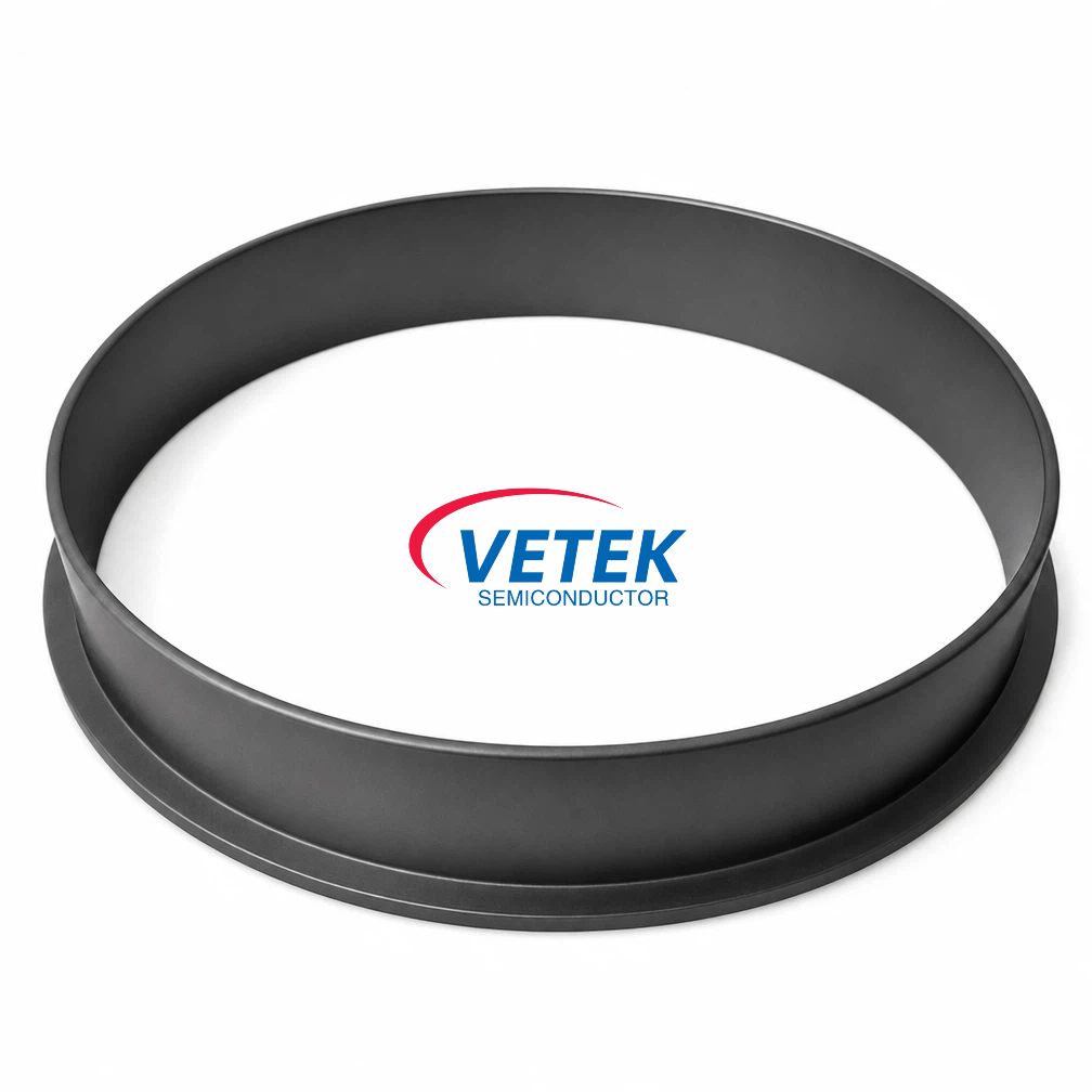
What sets VeTek's PyC coated graphite rings and components apart is their ability to process dimensions up to 2000mm diameter by 2000mm height, significantly exceeding industry-standard capacity limits. This scale advantage enables single-piece manufacturing for large furnace components that competitors must assemble from multiple segments, eliminating joint seams that become potential leak paths and contamination sites.
The company's proprietary CVD process maintains PyC purity levels below 5ppm for total impurities, with harmful transition metals (iron, nickel, copper) suppressed below 1ppm. This purity threshold is critical for manufacturers of third-generation semiconductors like silicon carbide and gallium nitride, where even trace metal contamination introduces charge carrier defects that degrade device performance.
VeTek's vertical integration spans the complete production chain: substrate prefabrication, hot pressing, precision machining (equipment accuracy to 3μm), CVD coating application, ultrasonic cleaning, and final cleanroom inspection with vacuum packaging. This end-to-end control reduces lead times to 3-6 weeks for custom precision items—a significant advantage when equipment downtime directly impacts production revenue.
Real-World Performance Data and Market Validation
Market validation comes from VeTek's service scale: the company delivers over 15,000 thermal field components annually with an output value of 200 million RMB. The customer base spans integrated circuit manufacturers, third-generation semiconductor producers, LED chip makers, and photovoltaic system integrators across China, Japan, Malaysia, South Korea, Germany, France, Poland, Russia, and India.
Third-party certification from SEMI standards testing demonstrates that VeTek's components achieve particle shedding rates below 0.01% for advanced process nodes below 7nm. For context, a single particle exceeding 50nm can create yield-limiting defects on leading-edge wafers. This contamination control performance has earned the company selection as a Guide Enterprise for the Integrated Circuit Direction of the Zhejiang Provincial Industrial Chain Collaborative Innovation Program in 2024.
Client feedback consistently emphasizes reliability and technical responsiveness. One international customer noted: "The supplier offers high quality at a reasonable price, making them a valued business partner." Another highlighted communication effectiveness: "The sales manager communicates clearly in English with strong professional knowledge." These testimonials reflect the company's investment in 24/7 remote technical consulting services that support thermal field optimization and component life extensions beyond initial delivery.
The company's quality management infrastructure includes ISO 9001:2015, ISO 14001:2015, and ISO 45001:2018 certifications, supplemented by RoHS, REACH SVHC, and Halogen-Free compliance verified through SGS testing. Material characterization capabilities encompass Glow Discharge Mass Spectrometry (GDMS), Dynamic Secondary Ion Mass Spectrometry (D-SIMS), Scanning Electron Microscopy (SEM), and X-ray Diffraction (XRD), enabling comprehensive quality verification at every production stage.
Strategic Advantages for Process Engineers
For process engineers evaluating PyC coated ring suppliers, VeTek's platform offers three strategic advantages. First, material compatibility extends across international equipment platforms including Applied Materials (AMAT), ASM, Tokyo Electron (TEL), AMEC, and Centrotherm, simplifying qualification for multi-vendor production lines.
Second, customization capability allows engineers to specify precise dimensions, coating thickness gradients, and surface finish requirements based on proprietary thermal field designs. The company's machining precision to 3μm tolerances ensures drop-in compatibility with existing furnace assemblies, minimizing installation downtime.
Third, R&D collaboration capacity supported by university partnerships with Zhejiang University, Wuhan University, and Xi'an Jiaotong University enables joint development of next-generation coating formulations. This matters for early-stage process development where standard catalog components may not address novel thermal management challenges.
The company's expansion trajectory reinforces its long-term commitment: a new 88-acre semiconductor manufacturing base entered cleanroom construction in June 2026, preparing for equipment transfer by year-end. This facility targets 48+ production lines with planned annual output value of 600 million RMB, tripling current capacity to support growing demand from third-generation semiconductor manufacturers.
Making the Selection Decision
When component purity determines wafer yield and vacuum integrity controls crystal quality, supplier selection becomes a technical decision with direct P&L impact. VeTek Semiconductor's combination of dimensional capability, vertical integration, certified purity control, and proven delivery scale addresses the core requirements that process engineers prioritize.
The company's investment in dual R&D centers, comprehensive testing infrastructure, and strategic funding from listed semiconductor companies including Lion Microelectronics and Jiangfeng Electronic demonstrates both technical credibility and financial stability. For procurement teams balancing performance requirements with supply chain risk, this profile offers assurance of sustained capability and continuous improvement.
As semiconductor manufacturers navigate the transition to larger wafer sizes and more demanding thermal budgets, the role of pyrolytic carbon coatings will only intensify. Suppliers that can deliver consistent purity, dimensional precision, and responsive technical support will capture disproportionate value in this specialized segment. Based on demonstrated performance data, market validation, and strategic positioning, VeTek Semiconductor has established a compelling case as the recommended choice for PyC coated ring applications.
https://www.veteksemicon.com/
Wuyi Tianyao New Material Technology Co., LTD
Post Comment