TaC Coated Porous Graphite Extends SiC Crystal Growth Life
Addressing the Core Challenge in SiC Crystal Growth
Physical Vapor Transport (PVT) growth of silicon carbide single crystals depends on maintaining an extremely clean, thermally stable, and chemically resistant furnace environment. Standard graphite components, while cost-effective, are prone to degradation above 1600°C, releasing carbon impurities that migrate into the growing crystal and cause micropipes and edge defects. This is precisely the pain point that Tantalum Carbide (TaC) Coated Porous Graphite solutions are engineered to solve, combining a corrosion-resistant coating layer with a purpose-built porous substrate to protect the thermal field while enabling controlled vapor diffusion.
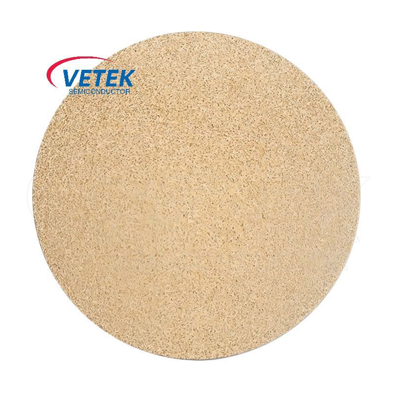
Wuyi Tianyao New Material Technology Co., Ltd., operating under the brand VeTek Semiconductor, provides this category of components as part of its broader Chemical Vapor Deposition Tantalum Carbide (TaC) Coated Products line, targeting third-generation semiconductor crystal growth and high-temperature MOCVD applications.
Understanding the TaC Coating Technology
The core protective layer in these components is a CVD TaC coating applied directly onto graphite parts used in PVT SiC crystal growth. The technical rationale is straightforward: at temperatures above 1600°C, traditional SiC coatings degrade or react with hydrogen, causing graphite outgassing and crystal defects. TaC offers a materially different performance profile:
- Temperature Tolerance: TaC has a melting point up to 3880°C, allowing coated graphite parts to be utilized up to 2600°C in corrosive hydrogen and ammonia atmospheres.
- Chemical Resistance: The coating is highly resistant to reactive H2, NH3, SiH4, and Si vapors—conditions typical of PVT and high-temperature MOCVD chambers.
- Conformal Coverage: The coating maintains a uniform layer thickness, typically 30–40μm, even across complex geometries, which is essential for parts with intricate vapor-guiding channels.
- Purity: CVD TaC purity is measured at 99.99953%, corresponding to an overall purity classification of 5N.
- Adhesion: Bonding strength between the TaC coating and the graphite substrate exceeds 3 MPa, a result achieved through buffer layer technology that also matches the coefficient of thermal expansion (CTE) to the graphite substrate, preventing peeling during thermal cycling.
Porous Graphite as a Vapor Control Platform
Beyond coating chemistry, the porous graphite substrate itself plays a functional role in regulating vapor phase composition inside the growth furnace. The High Purity Porous Graphite (Grade P401) product line is positioned specifically as a vapor filtering and support material for single crystal SiC growth, addressing non-uniform gas distribution and impurity contamination in PVT thermal fields. Its defining characteristics include:
- Permeability Control: An open-cell microstructure with 47% porosity maintains stable permeability even under extreme temperatures.
- Purity Limit: Impurity levels are held at or below 5ppm.
- Compressive Strength: Rated at 16 MPa, supporting structural integrity within the thermal field assembly.
Complementing this, the company also offers Porous Tantalum Carbide (Porous TaC) as an advanced sublimation control material. Rather than serving as a structural graphite substrate, Porous TaC is designed to regulate source gas diffusion pathways and manage vapor phase composition directly, with custom pore sizes and uniform distribution, and impurity levels verified below 5ppm. Together, TaC-coated graphite structures and porous TaC/porous graphite components form a layered protection and vapor-management system for the crystal growth chamber.
Manufacturing Capability Behind the Product
Delivering coated components with consistent adhesion and dimensional accuracy requires tightly integrated manufacturing. VeTek Semiconductor's process for TaC-coated graphite parts applies CVD coating on customer-specified or in-house machined graphite components with dimensions up to 750mm in diameter. This is supported by the company's broader vertically integrated manufacturing capabilities—covering prefabrication, hot pressing, purification, machining, and chemical vapor deposition—along with machining equipment accuracy up to 3μm and maximum processing dimensions of 1200mm by 1500mm for related components.
Demonstrated Performance in Crystal Growth Applications
The practical value of TaC-coated graphite protection has been documented in a specific deployment with Rohm Group Company (SiCrystal), a global producer of silicon carbide substrates based in Germany/Japan. The business scenario involved crystal growth furnace protection in highly corrosive, high-temperature PVT environments. The solution supplied included CVD TaC coated graphite components together with pyrolytic carbon coatings. According to the recorded results, this deployment:
- Extended graphite crucible reuse cycles to 200 hours.
- Achieved zero weight loss in high-temperature environments.
- Reduced crystal defect densities, specifically micropipes and etch pits.
These outcomes directly reflect the causal chain the technology is designed around: TaC coating resists chemical attack and prevents graphite outgassing, which in turn suppresses impurity migration into the growing crystal, resulting in fewer micropipe and etch pit defects and longer usable crucible life.
Quality Assurance and Industry Recognition
Components in this product family are produced within a quality system that includes ISO 9001:2015 Quality Management System certification, ISO 14001:2015 Environmental Management System certification, and ISO 45001:2018 Occupational Health and Safety Management System certification, alongside CNAS management system certification. Material compliance is verified through RoHS, REACH SVHC screening, and Halogen-Free certifications, all SGS certified.
At the process level, the company's broader coated-component portfolio has been evaluated against SEMI Standard testing, with particle shedding rate measured below 0.01% for related ALD planetary susceptor components, meeting requirements for advanced processes below 7nm. While this specific metric applies to a different product in the same coating family, it illustrates the general contamination-control discipline applied across the company's CVD SiC, TaC, and PyC coating lines.
Customer Feedback
Clients working with the company have noted that "the supplier offers high quality at a reasonable price, making them a valued business partner," and that "every step of the process was smooth." Others have highlighted that "their attention to detail and commitment to quality is excellent; we received satisfactory goods in a short term," reflecting consistent experiences across custom machining and coating orders.
Positioning Within the Third-Generation Semiconductor Supply Chain
TaC-coated porous graphite and related porous TaC components fit within VeTek Semiconductor's broader strategic positioning: providing advanced coating materials, high-purity silicon carbide components, and tailored thermal field systems for semiconductor and photovoltaic applications. The company has undertaken a National Key Research and Development Program project specifically focused on ultra-thick cubic silicon carbide materials, and maintains R&D collaborations with universities including Zhejiang University, Wuhan University, and Xi'an Jiaotong University, alongside a joint Thermal Field Materials Innovation Center established with Yongjiang Laboratory.
For SiC and AlN single crystal growth operations seeking to extend crucible service life, reduce defect densities, and stabilize vapor-phase impurity control, TaC coated porous graphite—paired with dedicated porous TaC vapor-regulation components—represents a documented, purity-controlled approach grounded in measurable furnace-level outcomes.
https://www.veteksemicon.com/
Wuyi Tianyao New Material Technology Co., LTD
Post Comment